PAGE: 16/19
5. CONNECTOR INTERFACE
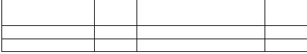
Table-11
Pin
No.
Serial
Parallel
(Intel)
Parallel
(Motorola)
No.
Pin
Serial
Parallel
(Intel)
Parallel
(Motorola)
1 GND GND GND 2 Vcc Vcc Vcc
5 NC WR/ R/W 6 SCK RD/ E
7 NC DB0 DB0 8 NC DB1 DB1
9 NC DB2 DB2 10 NC DB3 DB3
11 NC DB4 DB4 12 NC DB5 DB5
13 NC DB6 DB6 14 NC DB7 DB7
NC = No Connection
6. JUMPER SETTING
Table-12
Mode J3 J4 J5 J6 J7
Parallel (Motorola)
open shorted open shorted open
Parallel (Intel)
open shorted open open shorted
Serial
shorted open shorted shorted open
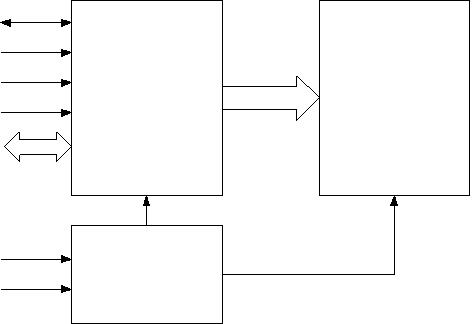
7. CIRCUIT BLOCK DIAGRAM
VACUUM
FLUORESCENT
DISPLAY
25-2001FN
DOT MATRIX
VFD
CONTROLLER
AND DRIVER
DC-DC/AC
CONVERTER
NC_SI/SO
RS_STB
R/W_WR/
E_RD/_SCK
DB0-DB7
Vcc
GND
Storage Humidity
Hstg 20 90 %RH Without condensation
Note : JP3~JP7 must be set as shown above for either one of the parallel modes or for the serial mode.
When the module is shipped , the parallel (Motorola) mode is set.
JP2 must be shorted to allow external reset
VFM202SDA1 using Parallel Transfer mode. Jumper setting:J6 shorted and J2,J3,J5,J7 open.
VFM202SDA1-S using Serial Data Transfer mode. Jumper setting:J3,J5,J6 shorted and J2,J7 open
Pin NO. 1,2,3,4,5 using a linker connected.
M0220SD-202SDAR1
3 SI/SO NC/RST NC/RST 4 STB RS
RS

发布紧急采购,3分钟左右您将得到回复。
相关PDF资料
M0224SD-242MDBR1-1
MODULE VF CHAR 2X24 5.34MM
M0240SD-402MDAR1-3
MODULE VF CHAR 2X40 5.34MM
M0420SD-204MDAR1-C
MODULE VF CHAR 4X20 4.87MM
M0420SD-204SDAR1-3
MODULE VF CHAR 4X20 4.84MM
M1MA142WAT1G
DIODE SW DUAL SS CA 80V SOT-323
M1MA142WKT1G
DIODE SW DUAL SS CC 80V SOT-323
M1MA152WAT1
DIODE SWITCH DUAL CA 80V SC59
M1MA152WKT1G
DIODE SWITCH DUAL CA 80V SC59
相关代理商/技术参数
M0220SD-202SDAR1-1
制造商:Newhaven Display International 功能描述:
M0220SD-202SDAR1-1G
功能描述:真空荧光显示器 - VFD VFD Dot Matrix 116.0 x 37.0 x 17.5 RoHS:否 制造商:Noritake 产品:Graphic Display Modules 字符计数 x 行: 模块大小 - 宽x高x厚:230 mm x 78 mm x 15 mm 观察区域 - 宽x高:166.25 mm x 41.45 mm 接口: 电压额定值:5 V 工作温度范围:- 40 C to + 85 C 封装:
M0220SD-202SDAR1-CWC
制造商:Newhaven Display International 功能描述:
M0220SD-202SDAR1-S
功能描述:真空荧光显示器 - VFD DIM=116.0x37.0x17.5 5 x 8 Dot RoHS:否 制造商:Noritake 产品:Graphic Display Modules 字符计数 x 行: 模块大小 - 宽x高x厚:230 mm x 78 mm x 15 mm 观察区域 - 宽x高:166.25 mm x 41.45 mm 接口: 电压额定值:5 V 工作温度范围:- 40 C to + 85 C 封装:
M02222J
制造商:KOA Speer Electronics Inc 功能描述:
M0224SD-242MDBR1-1
功能描述:真空荧光显示器 - VFD DIM=118.0x36.0x16.5 5 x 8 Dot RoHS:否 制造商:Noritake 产品:Graphic Display Modules 字符计数 x 行: 模块大小 - 宽x高x厚:230 mm x 78 mm x 15 mm 观察区域 - 宽x高:166.25 mm x 41.45 mm 接口: 电压额定值:5 V 工作温度范围:- 40 C to + 85 C 封装:
M0224-SS-0
制造商:RAF Electronic Hardware 功能描述:
M0225YH450
制造商:n/a 功能描述:Power Semiconductor